11.08.2025

Keywords: advanced packaging, semiconductor equipment, machine control software, chiplets, heterogeneous integration, warpage, metrology, systems engineering
The global advanced semiconductor packaging market (approximately $33.5 billion in 2025) is expected to almost double to approximately $62 billion by 2031.
The limitations of traditional transistor scaling are driving significant advances in the market, and therefore innovations such as chiplets, heterogeneous integration, and 2.5D/3D stacking are being developed to meet the future needs of AI, HPC, and advanced electronic applications.
However, as the industry expands the use of these technologies, it will become apparent that the teams approaching advanced packaging as a single–discipline problem will be left behind by those that can adapt to the multi-domain complexities of this technology.
The theme of embracing the multi-domain complexities of advanced packaging was addressed at the Swiss Semiconductor Day 2026.
Advanced packaging is located at the intersection of four distinct technical disciplines: thermal management, material science, mechatronics, and metrology.
Each discipline has its unique expertise and optimisation goals. The critical insight here is that each of the four domains cannot be optimised in isolation.
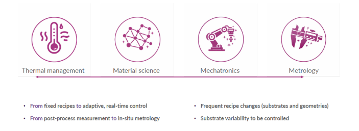
Warpage is one of the most difficult problems to solve in advanced packaging, especially when precision requirements and throughput are pushed to their limits, combined with the variability of substrates and geometries that often require recipe changes.
Although individual process steps are typically tightly controlled, some degree of variability always exists. Therefore, when operating near the limits of requirements, part of the solution is to measure and correct imperfections in real time during processing.
There are currently two major transitions underway in the industry. First, a transition from fixed recipes to adaptive, real-time control: as substrate variability and frequent geometrical changes become the norm, static process parameters are giving way to dynamic adjustments.
Second, a transition from post-process measurement to in-situ metrology: detecting defects or failures after they occur is too late in terms of cost and productivity when tolerances are very tight, and rework is costly.
Recent reviews on the subject confirm the complexity of this multi-disciplinary problem. For example, a 2025 review article published in Microelectronics Reliability emphasised that as semiconductor devices incorporate increasing levels of heterogeneous integration and 3D packaging, thermal management is becoming increasingly important for both device performance and reliability.
Advanced packages are currently approaching or exceeding an interconnect density of 1000 I/O/mm in silicon interposers, whereas conventional flip-chip designs typically contain only 48 I/O/mm.
This high-density interconnection structure severely restricts the available pathways for heat dissipation. Consequently, the necessity for thermally integrated and control-integrated strategies in advanced packaging is growing rapidly.
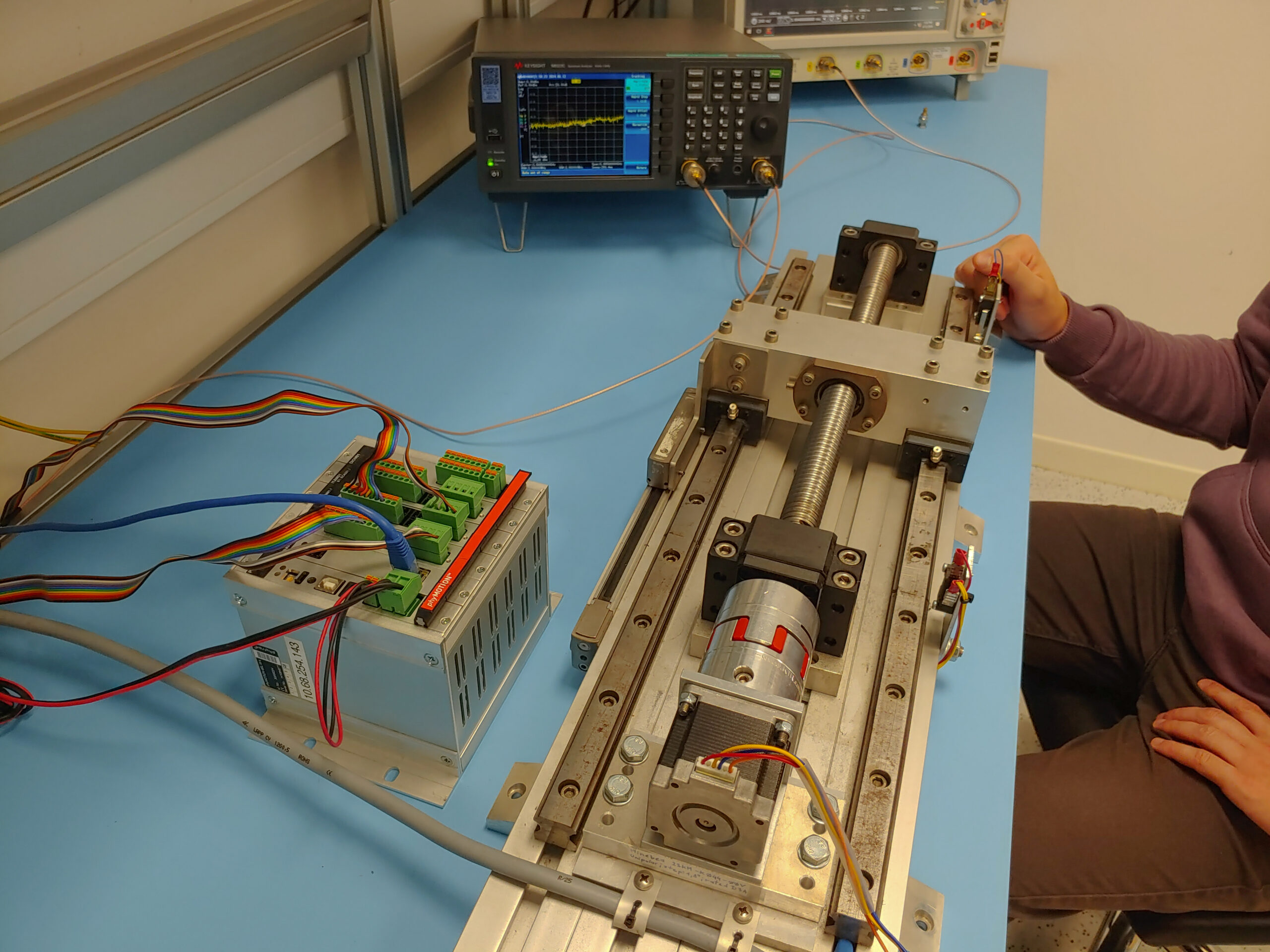
The mechanical subsystems of advanced packaging equipment are often the primary focus when developing such equipment. Precision stages, optical systems, vacuum chambers, and other subsystems are the visually identifiable components that determine a tool’s capabilities.
Engineering experience across many fields (semiconductor manufacturing, particle accelerator construction, medical devices, and plasma confinement for nuclear fusion) indicates that the mechanical subsystems are rarely the bottleneck when developing complex tools.
Rather, the optimal solution can be found through a combination of mechanical and software approaches, not through maximising mechanical capabilities. The mechanical capabilities are sufficient, but the control system is the limiting factor in determining the time to production.
Particularly for tools that require alignment accuracies better than a micron, very narrow process windows, direct coupling of vision and motion to throughput and yield, the control software becomes either an enabler or a constraint.
In other words, does the control architecture allow the tool to scale to increased complexity, or does it represent a ceiling that limits what the mechanical system can achieve?
A common thread runs throughout the industries, including semiconductor equipment original equipment manufacturers (OEMs) and scientific research facilities. Those customers who successfully navigate the most complex projects develop their project setup using teams that can apply systems thinking beyond their normal area of expertise, preferably down to the lowest possible level within the developer.
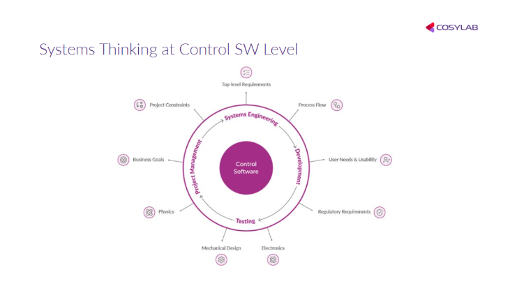
This is not just about employing generalists. It is about setting up team structures in which the software developer has a sufficient understanding of the physical and mechanical sciences to recognise when the optimal solution is to collaborate with experts from multiple disciplines.
It is also about having the mechanical engineer understand the limitations and constraints of controlling mechanisms well enough to design mechanisms that can be controlled deterministically. Finally, it is about recognising that in the case of advanced packaging, the interfaces between disciplines are where the most significant challenges to successful integration reside.
European countries can provide an excellent illustration of how ecosystems can create an environment for optimising complex applications. In contrast to large-scale manufacturing facilities where high-volume production is key to success, countries may develop a different value proposition. That value equation rests on the ability to provide custom solutions and the time needed to bring them into production.
This focus on complexity over volume is well-suited to the growth of advanced packaging. The tools used to enable chiplet integration, heterogeneous assembly, and 3D stacking are not commodity products. As the challenge’s complexity increases, the less likely it is that a standard product can meet it.
For example, OEMs working with semiconductor equipment need to identify suppliers capable of supporting both greenfield projects (end-to-end engineering for the creation of new tools) and brownfield projects (upgrading and adapting existing technology stacks and legacy systems).
Because the industry is constantly evolving, the ability to quickly develop reliable new solutions is nearly as important as the capability to develop them in the first place. In this context, value is defined by the combination of customisation and delivery speed.
In addition to being a multi-domain problem, the risks associated with integrating advanced packaging tools into semiconductor equipment pose many practical challenges for OEMs developing or upgrading such tools. Integration risk exists at three primary points along the development cycle, each with its own cost profile and potential solutions.
Pre-Design Freeze.
Working closely with one’s control system supplier and doing so as soon as possible is imperative. The sooner problems are identified during control system integration, the more options are available for solving them before the design freeze. Typically, late-stage firefighting on control-related issues results in schedule delays and costly rework, negatively impacting fab acceptance schedules.
During system integration.
Control architectures for advanced packaging tools typically require expertise across multiple domains, including PLC, FPGA, motion, vision, and data acquisition. Rarely do advanced packaging tools fit into a single control paradigm. The real-time nature of the deterministic timing requirements of the packaging process typically requires FPGA-level responsiveness. In contrast, the orchestration of the process and the flow of data requires greater coordination. When multiple specialities exist within a team or ecosystem, and no single person is accountable for integrating the overall system, the result is often integration gaps.
During fab acceptance.
One should plan for industrial readiness from the beginning. The gap between a functioning prototype and a production-ready, supportable tool is significant. Documented evidence of compliance, traceability and audit-readiness should not be considered as afterthoughts, as they will create technical debt that accumulates throughout commercialisation.
Advanced packaging is not a single-discipline problem; it is a systems engineering and control problem requiring tight integration among thermal management, materials science, mechatronics, and metrology.
Those teams and ecosystems that integrate these disciplines to the lowest possible level and apply systems thinking to the entire development process will generally outperform those that optimise individual domains independently.
The ability to move quickly is a competitive advantage. However, hurrying in the wrong direction, or moving swiftly on the component level while the integration of those components lags, is not an advantage.
For OEMs building advanced packaging tools, the question is not simply whether one has the mechanical precision or the process knowledge. The question is whether one’s project structure, team composition, and control-system supplier can tie those capabilities together into a working system.
For more information about Cosylab and its semiconductor solutions, visit www.cosylab.com.
Vintar, R. (2026) ‘Advanced Packaging: A Multi-Domain Engineering Problem’. Presentation delivered at Swiss Semiconductor Day 2026, Switzerland.
Kim, M., Kim, J., Park, W. and Kang, J.S. (2025) ‘A review in thermal management for advanced chip packaging from chip to heat sink’, Microelectronics Reliability, 170, p. 115782. Available at: https://doi.org/10.1016/j.microrel.2025.115782
Rok Vintar is a senior engineer at Cosylab, an engineering services provider for deep-tech projects, with expertise in semiconductors and system controls. He is also the Director of Business Development for the semiconductor equipment segment.
Rok has a unique perspective on what distinguishes successful development projects from prolonged integration cycles and missed production targets, drawing on his experience providing machine control systems for complex equipment across many years.