

Reduce Integration Risk While Protecting IP and Machine Control Availability
Reduce Integration Risk While Protecting IP and Machine Control Availability
8. July 2026
min read
Blog
Semiconductor
Semiconductor equipment design is increasingly developing at the boundaries between individual subsystems, teams and organisations. Although a module may meet all the tests required by its engineers, it will always have some risk of failure once installed in a larger system, such as the fab, because it was developed outside that environment.
Therefore, for OEM and Tier-1 supplier programme and development managers who need to plan and manage complex multi-project programmes, including managing their technical risks, the potential for integration issues across many different project streams is significant.
As such, they require ways to identify and isolate these types of risks, including compliance evidence, safety posture, interface maturity, and IP (intellectual property) exposure.
In our recent SEMICON Europa 2025 Industry Survey, we asked how many development managers were prepared to work with an engineering team external to their organisation. Although many respondents were prepared to do so, none stated they would do so until the external team met very strict trust conditions.
These included protecting IP, building fab readiness and compliance into their working methodologies, and requiring domain-specific expertise in semiconductor tool control that the external team had not simply acquired through “on-the-job” experience.
This blog post is part 3 of a three-part series examining what these trust conditions mean in practice.
Start from the beginning
To better understand the challenges discussed here, we recommend reading Part 1 of this three-part series.
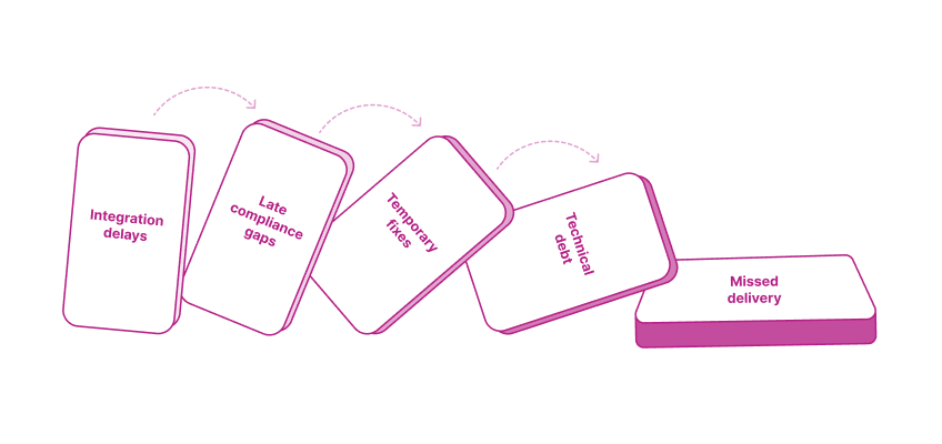
The risks in semiconductor equipment development are increasingly becoming integration risks. One module can be finished in isolation and yet fail when it connects to the other modules or even the fab itself.
The challenge for development managers is that integration risks don’t fit into a single project stream — they span multiple efforts, including supervision of compliance evidence, safety posture, and interface maturity.
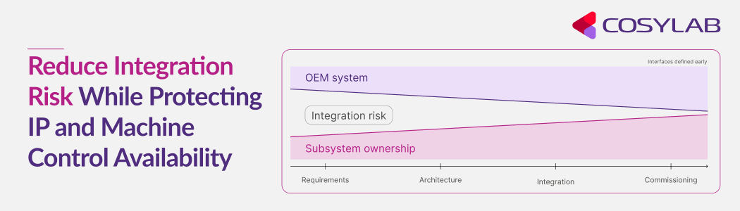
Additionally, these risks have to be addressed throughout the project’s lifetime, starting with requirements gathering and architecture design, and ending with commissioning.
Furthermore, the practical reality is that the final system will need to be supported under production constraints.
In our qualitative survey, sentiment was cautious but consistent. Respondents indicated an openness to collaborative engineering efforts with third-party vendors (embedded engineering teams) as long as “trust conditions” were satisfied.
The non-negotiables tend to be recognisable to anyone responsible for managing large-scale deliveries of tools. Third-party vendors must protect their clients’ intellectual property in a manner that can be supervised and enforced, not merely through contractual terms.
Third-party engineering teams must also support their client’s fab readiness and compliance disciplines by integrating them into the methodology for accomplishing the work, including safety expectations, traceability, and standards compliance, and by providing documentation that supports the qualification and auditing of the final system.
Furthermore, third-party vendor domain expertise in semiconductor tool control is not equivalent to generic software engineering, and “learning on the job” is rarely compatible with development critical timelines.
This is the area where Cosylab’s big science and industry heritage applies to semiconductor engineering services.
In safety-conscious, mission-critical environments where safety is paramount, and regulations govern the safe operation of systems, development teams learn to document all interfaces formally and to design control systems with limited access and staged commissioning.
All of these processes also help bridge prototype development into commercially viable products while eliminating the risk associated with integrating new components. These are precisely the same habits and methodologies that help bridge prototypes into production-ready tools without making integration a gamble.
What third-party embedded engineering team abilities make it eligible to support a development team?
- bridging prototypes to production-ready tools with compliant software control systems;
- supporting OEM customers with reliable engineering and flexible partnership arrangements;
- accelerating innovation, reducing risks, improving integration;
- possessing the reliability of an enterprise and the agility of a start-up;
- having proven themselves with Tier-1 semiconductor equipment OEMs.
The consistent message from our SEMICON Europa 2025 survey is clear: teams are willing to collaborate with external engineering partners when those partners bring domain expertise, protect IP and strengthen fab readiness, rather than creating additional coordination risk.
Reducing risk comes down to sequencing and boundaries. The earlier the project can establish subsystem ownership, the sooner it can define testing interfaces, and the sooner it becomes clear who will be responsible for verifying the correctness of these interfaces as they are integrated into a system.
As such, the grey area in which an issue bounces back and forth among multiple teams decreases significantly, and the predictability of system delivery increases.
Therefore, when programme managers evaluate whether to enter into a partnership with external engineering teams related to their semiconductor business, it is not the costs of such a relationship but rather trust that is the deciding factor.
The trust is predicated on demonstrating competency in the semiconductor industry, demonstrable IP protection, and disciplined practices that facilitate the qualification of partners from day one.
What to Read Next
Learn more about Cosylab’s semiconductor engineering services.
This is Part 3 of a three-part blog series. Read Part 1 on maintaining delivery speed under pressure, and Part 2 on relieving overloaded engineering teams.
Get in touch
Our team of experienced engineers is here to help. Let's discuss your project requirements and explore how our skillset can accelerate your turnaround.